 Skip to content
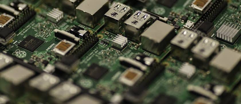
What is Shielding in Electronics?
Shielding in electronics is used to mean the practice where physical barriers are installed to reduce (or even eliminate) electromagnetic radiation or waves. This is also commonly called EMI shielding.
EMI can have many sources: power lines, electric equipment and systems, wireless communication devices and installations, or even natural occurrences like lightning and solar flares.
Electronics shielding involves the use of materials that can reflect or even absorb electromagnetic waves. This can be done on a small scale, or it can be a big shield that encloses electrical equipment and systems in a room.
Because EMI often affects electronic components and circuits, it becomes necessary to shield printed circuit boards. This is accomplished at both the design and assembly levels using various methods. Learn more about that below.
Resource: https://www.semanticscholar.org
PCB Shielding
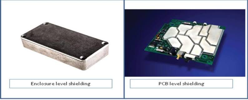
PCBs — or printed circuit boards in full — contain components and circuits that are susceptible to EMI. These must be protected, or the electronic system that has the PCB will not function as required. PCB level shielding is either aimed at preventing EMI in general or designed to shield against higher frequency waves of the radio wave level.
PCB EMI Shielding
PCB EMI shielding protects circuit boards from electromagnetic waves, and these can be low or high frequency. Low frequency interference sources include power lines and electrical appliances, while higher frequency sources are mostly wireless communication equipment or devices and installations.
PCB RF Shielding
PCB RF shielding refers to the use of physical barriers that protect circuit boards against the effects of radio frequency waves. Radio waves are those whose frequencies range from 3 kHz on the lower scale to 300 GHz on the higher end.
An RF PCB shield is mostly used in the high-frequency circuit boards of wireless electronic devices and systems. These can be broadcasting or communication equipment and receiving devices. PCB RF design shielding — or that of EMI in general — can take many forms, as discussed next.
Resource: https://www.semanticscholar.org
PCB Shielding Techniques
A PCB shield can be a shield to protect the circuit board from external interference, a shield to prevent the board from becoming a source of EMI itself, or a shield to protect parts of the board from interfering with one another.
In light of that, PCB shielding techniques today include the following: shielding cans, solid copper layers, shielding film, shielding ink, and PCB gaskets.
PCB Shielding Cans
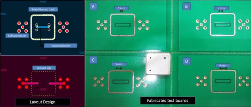
PCB shielding cans are solid metal enclosures that engineers use isolate parts of a circuit board or its entire area, most of the time with the aim of protecting delicate circuits or components. Different metals are used for this type of shield with stainless steel being one of the most common.
A PCB shielding can works by forming a Faraday cage around electric or electronic components. Upon striking the cans surface, EM waves generate currents in the metal, and these are safely dissipated to ground.
These enclosures can also help keep radiation inside the enclosed space, preventing it from interfering with other PCB components or nearby electronic circuits. PCB shield design, when it comes to cans, is widely varied and the enclosures can be any shape.
PCB Shielding Copper Layer
The addition of copper layers is one of the most used PCB shielding techniques. Also, the most effective when it comes to PCB shields. These layers are solid pieces of copper sheet that connect to ground via openings in the board, and may be solid planes or crosshatched.
Solid copper PCB shield is preferred when flexibility is not a major concern, and crosshatched when the board needs to flex. But while a crosshatched shield allows for flexibility, it also reduces the shields overall effectiveness, and should not be used unless needed.
Shielding PCB circuit boards using copper layers is a good choice for high density circuit boards. It also allows for controlled impedance and can be used in both rigid and rigid flex applications. That said, this shield is also the most expensive option.
PCB Shielding Film
PCB shielding film is a three layer film that engineers use when the flexibility of the shield is a major requirement. This shield consists of an upper insulation made of epoxy material, a middle metal deposition layer (to allow for easier attachment to surfaces), and an adhesive backing.
When compared to other PCB shielding techniques, films offer more flexibility and can be used on a broad range of surfaces, including curved ones and corners. It’s also an economical solution, seeing that it only requires few steps to both produce and apply.
You can use shielding film on both rigid and flex circuit boards, regardless of whether they require controlled impedance or not. However, owing to their slippery nature, these shielding films can make attaching stiffeners difficult.
PCB Shielding Ink
This is a silver-based ink that can absorb the energy of electromagnetic waves and prevent them from causing interference. Most often, this PCB EMI shield is applied automatically, using robotic spray nozzles, or it can be manually applied using a brush.
EMI shielding ink offers greater flexibility than other PCB level shielding methods and you can use it on any type of board surface. However, it presents one of the most expensive PCB shielding techniques available today, given that it requires more application steps such as curing.
When using PCB shielding ink, impedance can be difficult to control, and this is one of its downsides. It’s also not as effective as the shielding methods that involve solid materials, although thicker layers may be used.
PCB shielding Gasket
A PCB gasket is a flexible type of shielding material that’s typically made of conductive foam and sometimes rubber. The foam is made conductive by impregnating it with metal or carbon particles, which makes it an absorptive type of EMI shield.
PCB shielding gaskets may also be wrapped with conductive fabric, in addition to being conductive themselves. They come in useful when openings that might leak or allow electromagnetic waves into a space must be sealed off.
In addition to offering a cost effective way to shield PCB components and circuits, the EMI gasket presents a material that can be easily cut or shaped. These shields will also often come with adhesive surfaces to make sticking them to PCBs easier.
Conclusion
With many EMI sources around electrical and electronics systems today, PCB shielding is not only necessary but also a product quality requirement. EMC regulations also require that too, especially where the radiation from electronic devices must be controlled.
The PCB shielding techniques discussed in this post explain the ways that manufacturers are using various methods to prevent circuit boards from radiating EM waves and, more importantly, protect them against external radiation.